Electrons in Lithography and Imaging for Science and Application
16.-19. NOVEMBER 2026
STYKKISHÓLMUR, ICELAND
Scientific Scope
ELISA 2026 spans the full landscape of electron-based science and technology, from the fundamental processes that govern electron–matter interaction to the instruments and applications that translate this understanding into imaging, patterning, and nanomanufacturing.
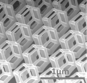
Rapid advances in beam technologies, resist materials & precursors, and data- / feedback-driven control are redefining how we understand and exploit electron-matter interactions. By merging the traditions of LE2AP, LEELIS and FEBIP, the meeting creates a unified space where modelling, metrology, experiments, and instrumentation converge – bridging physics and fabrication, materials and devices, and concepts and implementation. This perspective maintains the LE2AP+LEELIS initiative while including multi-material, hybrid 3D nanostructures central to the Beam Induced Nano-Manufacturing community.
The meeting fosters dialogue between foundation science and applications, strengthens bridges across core disciplines, and promotes shared terminology, metrology and benchmarking. It encourages collaboration among academia, industry, and instrument developers, offers visibility and networking.
Importantly it offers continuity as an excellent platform for early-career researchers and students for interaction with established academic research groups and industry, and helps shape a collective vision for next-generation electron-based science and technology.
Thematic Pillars
The topics below are representative rather than exhaustive. Related or emerging concepts in electron-based science, lithography, imaging, and nanomanufacturing are equally welcome.
Fundamentals of Electron–Matter Interaction
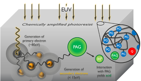
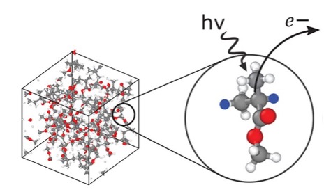
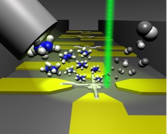
Generation of electrons in photon-, electron-, ion-, or atom-beam environments
Transport, absorption, scattering, and energy dissipation in solids and soft matter and charging in insulating materials
Low-energy electron induced chemistry in molecular precursors and resist materials
Theory, modelling and simulation of electron-induced processes.
Methods & Instrumentation
Extreme Ultraviolet and X-ray lithography.
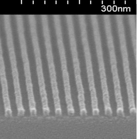
Electron-, ion- and atom-beam lithography.
Advanced light and beam sources, and detector systems.
Low-voltage and high-resolution electron microscopy (e.g. LEEM, SEM, STEM, CDSEM).
Cryo-based platforms for soft and hybrid materials.
Metrology, tools, methods and measures.
Correlative spectroscopy (e.g. photoemission, IR, RGA, MS, tomography)
Hybrid approaches combining electrons, ions, and photons for multimodal analysis.